
The Illusion of In-House Silicon
Microsoft, Google, Meta, and Amazon. What do these four companies have in common? At this very moment, they are paying billions of dollars in “taxes” to Nvidia’s Jensen Huang, while secretly working behind the scenes to build their own “Nvidia killer” custom silicon. Google boasts about its TPU v5p architecture, Microsoft unveils its Maia 200, and Meta continuously hypes the next-generation MTIA chips, telling the press that Nvidia’s hardware monopoly is about to end.
Do not be fooled by this grand charade. Today, we look past the meticulously crafted PR press releases and dissect the brutal, data-backed truth: the astronomical physics of hardware design costs and the impenetrable trap of Nvidia’s software ecosystem.
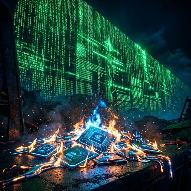
Image: Custom Silicon dreams melting against the impenetrable wall of Nvidia’s software ecosystem.
1. The $100 Million Tape-Out Barrier: The Brutal Physics of TSMC
Many stock market investors naively assume that because Nvidia commands profit margins exceeding 80% on each GPU, tech giants could save tens of billions simply by printing their own hardware. However, semiconductor physics and manufacturing economics are brutally unforgiving. Drawing a chip structure on a spreadsheet is free; manufacturing it physically means bowing down to the supreme power of TSMC’s cutting-edge foundries.
Let’s expose the latest 2026 Foundry pricing data. Back in the golden age of the 28nm node, a single silicon wafer cost roughly $5,000. Today, the cutting-edge TSMC 3nm wafers—used by Nvidia’s Blackwell and the highest-tier custom silicon from Big Tech—have skyrocketed to staggering prices between $18,500 and $20,000 per wafer. The upcoming 2nm wafers are already confirmed to hit a jaw-dropping $30,000.
Even more brutal is the initial sunk cost, known as the “Tape-out Cost.” Just to design a 3nm architecture and carve the initial testing masks, a company must burn a minimum of $100 million in pure cash. If a catastrophic bug is discovered in the design? That entire $100 million is incinerated, and you must start over. Moving forward, the projected platform development cost for a 2nm system sits at roughly $725 million in R&D.
While cash-rich monsters like Google and Microsoft can technically afford to burn this capital, the real tragedy lies in timing. By the time they spend 2-3 grueling years to finalize an in-house chip, secure TSMC allocation, and rack them into data centers, Nvidia has already unveiled its next-generation monster architecture (e.g., Rubin), laughing at their obsolete specs. The custom silicon race is a muddy trench war where Nvidia controls both the clock and the manufacturing levers.
2. AMD’s Achilles Heel: Saving Millions on Hardware, Losing Millions on Overtime
If building custom chips is pure hell, why not buy massive quantities of instinct MI300X or MI325X from AMD, the number two market player? On paper, AMD’s hardware specs obliterate Nvidia’s equivalent H100s. They boast significantly larger memory bandwidth and come at nearly half the price. It seems like a no-brainer.
Yet, cold, calculating cloud providers are still agonizingly hesitant to adopt them. The reason? A desperately fragmented software stack known as ROCm. Throughout 2025 and 2026, AMD pushed ROCm 6.2, adding crucial features like FP8 support and vLLM integration. But the reality on the ground from AI developers remains incredibly harsh.
In Nvidia’s CUDA environment, PyTorch training codes run flawlessly with a single click. In the ROCm ecosystem, unoptimized generic kernels often cause severe bottlenecks or random memory crashes. Consequently, highly paid elite AI engineers—who should be improving model performance—spend agonizing nights scouring GitHub issue threads and legacy StackOverflow posts to rewrite compatibility codes. The money saved on cheap hardware drains directly down the sink of astronomical developer payrolls and devastating project delays.
3. The 15-Year CUDA Trap: Silicon is Just a Rock; Software is the Soul
To truly understand this structural contradiction, observe the factual comparisons below.
| Metrics | Nvidia (H200, Blackwell) | Broad GPUs (AMD MI300X) | Big Tech Custom Silicon (TPU, Maia) |
|---|---|---|---|
| Software Ecosystem | CUDA (15-yr matured standard. 90%+ share) | Fragmented ROCm causing high debugging difficulty | Closed ecosystems forced (JAX, XLA) |
| Manufacturing & Capex | Secures TSMC’s top VIP allocation out of sheer profit margins | Limited by advanced packaging (CoWoS) constraints | Initial TSMC 3nm Tape-out burns $100M+. ROIs are impossible. |
| Day-1 Compatibility | Instant Day-1 optimization for the latest models | Delayed support resulting in generic, slow PyTorch fallbacks | Zero broad compatibility; strictly limited to internal proprietary use cases |
The true wellspring of Nvidia’s astronomical profits, the CUDA platform, was first deployed back in 2007. For over 15 tortuous years, graduate students and researchers globally have compounded millions of lines of code and research papers exclusively atop the CUDA ecosystem. Every genius entering the AI industry today speaks CUDA as their “first language.”
Ask yourself: How would you react if your boss ordered you, “Because AMD chips or our new internal NPUs are cheaper, throw away the mother-tongue (CUDA) you’ve mastered over the past ten years, and rewrite this massive AI model from scratch using a completely unfamiliar foreign language (ROCm, JAX) starting today?”
This is exactly why cash titans like Apple and Google, despite dumping tens of billions of dollars, cannot even scratch Nvidia’s toenail in the broader cloud AI market. Nvidia did not just build good hardware; they rewired the neuronal coding habits of every software engineer on the planet.
4. Conclusion: The Leash Won’t Break, It Only Stretches
Countless financial YouTubers and sensational tech journalists desperately pump out headlines screaming, “Big Tech’s Custom Silicon Finally Shakes Nvidia’s Throne!” to farm clicks. However, the cold, unforgiving manufacturing data from TSMC in 2026, combined with the visceral anger of on-ground developers, proves these narratives are complete fiction.
Custom in-house silicon is merely a desperate “cost-mitigation tool” utilized by Big Tech to squeeze out marginal efficiency inside their specific internal algorithms. It is not the Excalibur that will destroy Nvidia’s 15-year-old global AI infrastructure empire. For the foreseeable future, tech giants will swallow their pride, endure their bleeding bank accounts, and quietly pay whatever TSMC wafer price hikes Jensen Huang decides to pass on.
(However, even this seemingly eternal monolith shows microscopic fractures. What happens when computing power shifts away from fire-breathing cloud data centers and directly into the devices in our pockets—the explosive rise of the Local NPU Inference Market? Will this be the catalyst that finally brings the empire to its knees? Find out in Episode 3: ‘Breaking the Leash’.)
Sources & References
- TSMC Wafer Pricing & Tape-Out Costs: Data modeling and foundry pricing projections (28nm to 2nm) curated from extreme manufacturing cost reports by Tom’s Hardware, Notebookcheck, and Techspot (2025-2026).
- AMD ROCm Software Frustrations: Aggregated developer experiences, PyTorch fallback issues, and ecosystem fragmentation reported across GitHub issue trackers, TechPowerUp, and r/MachineLearning.
- Big Tech Capex & AI Custom Silicon: Analysis of Microsoft (Maia), Meta (MTIA), and Google (TPU) R&D expenditures derived from SEC filings and 2026 Capex projections (SeekingAlpha, Business Insider).