
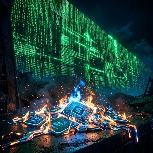
Microsoft, Google, Meta, and Amazon. What do these titans have in common? At this exact moment, they are paying tens of billions of dollars in extortionate “taxes” to Nvidia, while desperately funneling cash into secret, behind-the-scenes labs to build their own “Nvidia-killer” custom silicon chips. Google parades its TPU v5p; Microsoft flexes its Maia 200 architecture; Meta continually hypes the MTIA chip line—all feeding a single media narrative: “Nvidia’s hardware monopoly is about to end.”
Do not be fooled by perfectly crafted PR statements. Today, we rip off the band-aid and expose the brutally honest, data-backed reality. The dream of “in-house silicon” is melting against the impenetrable physics of modern semiconductor manufacturing costs and the unbreakable curse of Nvidia’s software ecosystem.
1. The $100 Million Tape-Out Barrier: The Brutal Economics of TSMC
Mainstream stock investors suffer from a critical illusion. They deduce that because Nvidia commands an 80% profit margin on its GPUs, a tech giant building its own chip will magically save billions. However, drawing a chip layout on a whiteboard is virtually free; actually physically manufacturing it means surviving the extortionate, monopolistic pricing of TSMC’s cutting-edge foundries.
Let’s examine the raw 2026 Foundry facts. Back in the golden age of the 28nm node, a single silicon wafer cost a modest $5,000. Today? The cutting-edge TSMC 3nm wafers—the exact nodes required for Nvidia’s Blackwell and Big Tech’s highest-tier custom silicon—have brutally skyrocketed to between $18,500 and $20,000 per wafer. Looking just around the corner, 2nm wafer pricing is officially projected to hit a staggering $30,000.
But wafer prices are just paper cuts compared to the real financial hemorrhage: the Tape-Out Cost. Just to engineer a 3nm architecture and fabricate the initial test masks, a company must immolate a minimum of $100 million in upfront cash. If testing reveals a fatal hardware bug? That $100 million goes up in smoke, and you must print the masks all over again. Moving to the 2nm paradigm requires platform development budgets soaring past $725 million.
Sure, Microsoft and Google can afford to burn this kind of capital. But here is the tragic punchline: By the time they spend 2 to 3 agonizing years designing an in-house chip, begging TSMC for production capacity, and racking them into data centers, Nvidia simply unveils its next-generation architecture (like the Rubin architecture). The new Nvidia chip instantly offers double the performance, rendering the multi-billion-dollar custom silicon project instantly obsolete. It is a rigged game where Nvidia controls the clock.
2. AMD’s Achilles Heel: Saving Millions on Hardware, Bleeding it on Overtime
If building custom silicon is a financial death trap, why not pivot and buy AMD’s powerful Instinct MI300X or MI325X chips? On paper, AMD’S hardware is nothing short of a miracle. The MI300X boasts larger memory bandwidth than the Nvidia H100 and sells for barely half the price. It seems like the ultimate no-brainer solution to the AI ROI crisis.
Yet, the world’s sharpest cloud providers are fundamentally terrified of adopting them en masse. The culprit? An agonizingly fragmented software stack called ROCm. Throughout 2025 and 2026, AMD has valiantly pushed updates like ROCm 6.2, fighting tooth and nail to optimize crucial elements like FP8 and vLLM. But the reality down in the developer trenches is a different story.
In Nvidia’s tightly guarded CUDA environment, PyTorch training codes execute flawlessly with a single click. Conversely, in the ROCm ecosystem, unoptimized generic kernels frequently trigger severe computational bottlenecks or catastrophic systemic memory crashes. Consequently, highly paid elite AI engineers—professionals who earn $300K+ a year to build neural networks—spend their miserable nights scouring GitHub issue trackers and ancient Reddit threads, hacking together compatibility patches. The millions of dollars supposedly “saved” by buying cheaper hardware immediately vanishes down the drain of skyrocketing developer payrolls and crushing project delays.
3. The 15-Year CUDA Moat: Silicon is Just Sand; Software is the Soul
To crystallize this massive structural contradiction, let us visually dissect the true nature of this monopoly.
| 🔍 Analytical Metric | 🟢 Nvidia (H200, Blackwell) | 🔴 Broad GPUs (AMD MI300X) | 🔵 Tech Custom Silicon (TPU, Maia) |
|---|---|---|---|
| 🧠 Software Ecosystem | CUDA (15-year standard. 90%+ share) | Fragmented ROCm; extreme debugging difficulty ⚠️ | Closed ecosystems (JAX, XLA) forced upon engineers 🚫 |
| 🏭 Manufacturing Cost | Secures TSMC VIP allocation via pure profit mass | Struggles with advanced packaging (CoWoS) bottlenecks📉 | Incurs $100M+ per 3nm tape-out upfront. Fatal ROI. 💸 |
| ⚡ Model Compatibility | Instant ‘Day-1’ PyTorch optimization & bug support ✨ | Persistent fallback delays on major updates ⏳ | Zero external compatibility. Trapped internally. 🔒 |
Nvidia’s true crown jewel, CUDA, was unleashed upon the world back in 2007. For over 15 years, globally distributed researchers and graduate students have compounded tens of millions of lines of code exclusively on CUDA. Any young artificial intelligence genius entering the market today speaks CUDA as their absolute “mother tongue.”
Put yourself in their shoes. If an executive orders you: “We bought these new custom AMD/NPU chips to save money. Go throw away your 10 years of CUDA fluency and rewrite our entire multi-billion-parameter LLM from scratch in this buggy, undocumented new language,” how would you react? This is precisely why Apple, Amazon, and Google fail to dethrone Nvidia in the open cloud market despite possessing unlimited cash reserves. Nvidia didn’t just win the hardware race; they successfully hijacked the neural pathways and coding habits of the entire human developer base.
4. Conclusion: The Silicon Leash Cannot Be Broken, Only Stretched
Financial YouTubers and desperate tech journalists will continue to publish clickbait declaring the “End of Nvidia” every time a tech giant announces a new proprietary chip. But the cold, physical limits of TSMC’s manufacturing economics combined with the furious exhaustion of real-world developers prove these “end-of-empire” narratives are pure fiction.
Custom silicon serves merely as a hyper-specific, internal “cost-mitigation tool” utilized to shave marginal percentages off specific internal data crunching. It is not the silver bullet that slays Nvidia’s globally entrenched AI infrastructure empire. For the foreseeable future—and barring a paradigm shift—the tech titans will continue to swallow their pride, watch their bank accounts hemorrhage, and dutifully pay whatever exorbitant wafer tax Jensen Huang demands.
🔗 Sources, Fact-Checks & References
- TSMC Wafer Pricing: Foundry pricing and Tape-out cost modeling (Tom’s Hardware, Notebookcheck, 2025/2026 data).
- AMD ROCm Software Frustrations: Aggregated PyTorch fallback issues from GitHub (ROCm) and TechPowerUp ecosystem analysis.
- Big Tech Capex: Financial expenditures derived from official corporate Capex projections via Seeking Alpha.